India is poised to join the exclusive group of nations equipped with Extreme Ultraviolet (EUV) lithography machines, which are currently produced solely by ASML, a company based in the Netherlands. This advanced technology has only been supplied to major players such as TSMC in Taiwan, Samsung in South Korea, and Intel in the United States. Meanwhile, Russia is expected to become the second nation to design and develop its own EUV machine, while China is making significant national efforts to achieve this technological milestone. The production of advanced semiconductors and the lithography machines that create them have become critical technologies, leading to heightened geopolitical tensions, particularly between the U.S. and China. The U.S. has imposed restrictions on the export of EUV lithography machines to China as part of broader trade policies aimed at limiting China's capacity to develop cutting-edge semiconductor technology for military and technological supremacy.
ASML's EUV lithography machine is the only one in existence capable of precisely etching billions of transistors onto a 30-centimetre wafer. In response to this technological gap, China is reportedly undertaking a national initiative to develop its own version of the machine, a project that has been likened to the Manhattan Project in Western technology circles. The EUV lithography machine can produce semiconductor chips at the nanoscale, measuring nearly a thousand times thinner than a human hair. These chips serve as the foundational elements for various advanced technologies, including artificial intelligence, mobile devices, space exploration, defence systems, clean technology, and consumer electronics.
Possessing the capability to manufacture these minuscule chips is essential for any nation or multinational corporation aiming to establish itself as a global economic and military power. The ability to produce advanced electronic components and sophisticated weapon systems is increasingly linked to the mastery of semiconductor technology. As countries like India and China strive to secure their positions in this critical field, the race for technological supremacy continues to intensify, underscoring the strategic importance of EUV lithography in the modern, highly industrialised world.
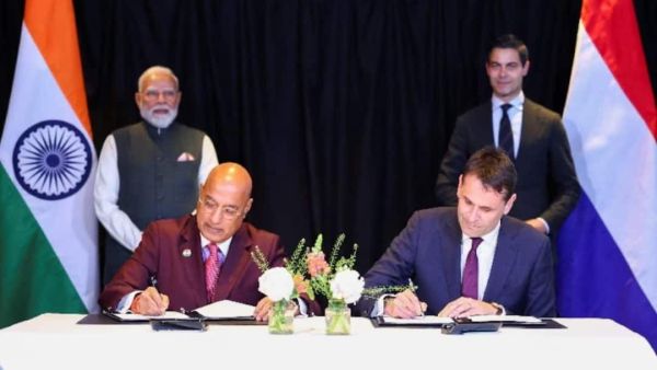
In this backdrop, the announcement by India's Tata Electronics regarding the conclusion of a partnership deal with ASML to establish a photolithography machine marks a significant step in the development of an $11 billion semiconductor facility in Dholera, Gujarat. This agreement was unveiled during Indian Prime Minister Narendra Modi's visit to the Netherlands on May 16. The introduction of this lithography machine is not merely a technological advancement; it represents a strategic asset, as it is controlled by a limited number of non-Chinese entities. This machine serves as both a commercial catalyst for enhancing the nation's economic capabilities and a crucial element for achieving strategic autonomy.
The collaboration between Tata Electronics and ASML occurs in the context of a global push by various countries to diversify their semiconductor supply chains and reduce dependence on specific manufacturing hubs. This initiative transcends the establishment of a conventional manufacturing plant; it signifies India's ambition to become a key player in one of the world's most advanced technological sectors. By engaging in this partnership, India aims to position itself prominently within the global semiconductor landscape.
A pivotal aspect of the Dholera facility will be the production of 300 mm semiconductor wafers, which are recognised as the global standard for semiconductor manufacturing. These wafers, thin silicon discs essential for fabricating microchips and integrated circuits, offer significant advantages in production efficiency. The larger size of 300 mm wafers allows semiconductor manufacturers to generate a higher volume of chips within the same production cycle, thereby enhancing cost-effectiveness through improved economies of scale. Furthermore, a substantial proportion of chips utilised in AI servers, data centres, smartphones, and next-generation vehicles are based on 300 mm wafers.
This significant agreement marks India's rise as a reliable participant in the Western technology supply chain, a development crucial for the country's economic transformation and geopolitical standing. It plays a vital role in advancing India's semiconductor aspirations, which carry important implications for the nation's technological alliances.
The strategic partnership with the Netherlands will facilitate India's access to the world's most advanced photolithography machines and tools, essential for producing nanometer-scale semiconductor chips. India’s semiconductor ecosystem will get a huge fillip with ASML, holding a global monopoly on these machines, making it the sole supplier. The cost of EUV lithography machines ranges from $150 million to $ 400 million, underscoring the investment required for this technology.
The collaboration between Tata Electronics and ASML aims to implement ASML's comprehensive suite of advanced lithography tools at the Dholera fabrication facility. This partnership is expected to enhance the operational efficiency of India's first commercial 300 mm semiconductor fab, ultimately benefiting Tata Electronics' clientele. Additionally, both companies will work together to cultivate domestic talent, strengthen the supply chain, and promote research initiatives to ensure the long-term viability of the Dholera fab. As semiconductors become increasingly integral to modern economies, India's semiconductor mission, established in 2021, reflects a growing recognition of the importance of these critical components, with hopes of achieving self-sufficiency in a market currently dominated by Taiwan, China, South Korea, and the United States.
As noted earlier, the ability of a country to produce semiconductors hinges significantly on a single machine known as EUV Photo Lithography. Amid the escalating technological rivalry between the United States and China, the U.S. government took an extraordinary step by threatening to instruct the Netherlands to cease the supply of lithography equipment to Chinese semiconductor companies. Such a move would have dealt a severe blow to China's semiconductor industry, with far-reaching implications for its economic future.
In response to this threat, China accelerated its efforts to develop its own lithography machines, launching a national initiative reminiscent of the Manhattan Project during World War II. This highly secretive U.S. endeavour ultimately led to the development of the atomic bomb. Similarly, China aimed to achieve self-sufficiency in lithography technology by reverse engineering the machines and enticing Chinese technicians from ASML, a leading lithography company, to return home. Reports indicate that China has made significant strides in this area and anticipates producing its first domestically manufactured lithography machine by the end of the decade, thereby reducing its reliance on Dutch and American suppliers.
The export restrictions on EUV technology and lithography machines to China highlight the strategic importance of ASML within the global technology landscape. Meanwhile, India's strengthened strategic partnership with the Netherlands has enabled Tata Electronics to acquire this complex machinery from ASML, showcasing how geopolitical relationships can influence access to critical technology.
-
Over 21,000 candidates qualify in Telangana DEECET 2026

-
Telangana TOSS results 2026: Girls lead, overall pass rates rise significantly

-
US disables another ship headed for Iran despite blockade

-
PSG wins back-to-back Champions League titles after shootout victory against Arsenal

-
India’s vultures are coming back, one tiger reserve at a time